what is wafer dicing
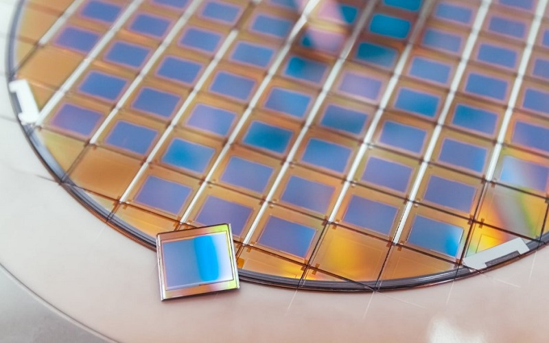
Wafer dicing, also known as wafer sawing or die singulation, is a critical process in semiconductor manufacturing. It involves the cutting of a semiconductor wafer into individual chips, each containing one or more integrated circuits (ICs) or electronic components. The primary purpose of wafer dicing is to separate the multiple devices that have been fabricated on a single wafer into discrete, functional units that can be further processed and packaged. Here are the key aspects of wafer dicing:
1. Purpose: The primary purpose of wafer dicing is to transform a single semiconductor wafer, which contains multiple integrated circuits or devices, into individual chips or dice. Each chip can then be packaged and used as an individual electronic component.
2. Semiconductor Wafers: The starting material for wafer dicing is a semiconductor wafer, typically made of silicon. These wafers are circular, flat substrates on which ICs are fabricated during the semiconductor manufacturing process.
3. Methods: There are two main methods of wafer dicing:
- Blade Dicing: In blade dicing, a thin, high-speed rotating blade, often embedded with abrasive particles, is used to mechanically cut the wafer along predefined lines or scribe lines.
- Laser Dicing: Laser dicing employs a high-energy laser beam to ablate and separate the material along the cutting path. It is a non-contact method and is suitable for delicate materials and precise cuts.
4. Quality Control: Precision and quality control are crucial in wafer dicing to ensure that the individual chips meet the required specifications. Inspection and measurement techniques are employed to verify dimensions, alignment, and quality.
5. Equipment: Specialized dicing equipment, such as dicing saws for blade dicing and laser dicing machines for laser dicing, is used for this process. These machines are equipped with precise control mechanisms to ensure accurate cuts.
6. Scribing: Before dicing, scribe lines are created on the wafer’s surface. These lines serve as guides for the dicing process, ensuring that the cuts are made precisely according to the design specifications.
7. Post-Dicing Cleaning: After dicing, the individual chips are typically cleaned to remove any debris, particles, or residues left from the dicing process. Clean chips are essential for reliable packaging and assembly.
8. Packaging: Once the chips are diced and cleaned, they are placed into semiconductor packages, which provide electrical connections, protection, and mechanical support for the chips. The type of package used depends on the specific application.
9. Testing: Packaged chips undergo electrical testing to ensure they function correctly. Testing may include functionality tests, parametric tests, and other quality control measures.
10. Applications: Diced chips find applications in a wide range of electronic devices, including microprocessors, memory chips, sensors, integrated circuits, and more.
In summary, wafer dicing is a crucial step in semiconductor manufacturing that involves cutting a semiconductor wafer into individual chips, which can then be packaged and used in electronic devices. It requires precision, quality control, and various methods to achieve the desired results.